Effect Pedal Circuits, Electronic Components, Electronics Tutorials, Transistors
Electronics Tutorials: the JFET (II) – Circuit analysis
In the first JFET post we presented this semiconductor device along with its basics, like the gain, principle of operation and working regions. Now you’re ready to dig into the analysis of some of the circuits you can find in effect pedal kits like our JFET buffer!
For the next sections we’ll use some of the concepts we explained in the previous post, like the characteristic curves of the transistor, so be sure to check it out if you have any trouble.
1 – JFET DC Biasing
One very important concept when designing JFET based amplifiers is to remember that these devices must be biased. What does that mean? As it happens with BJT transistors, you can’t just connect your guitar output to a transistor and expect it to work! You have to define a “sweet spot” by using some external parts where the transistor can work correctly as expected. This is also known as working point or Q-point of the transistor.
To better understand this concept we’ll analyse our first JFET circuit: the common source configuration.
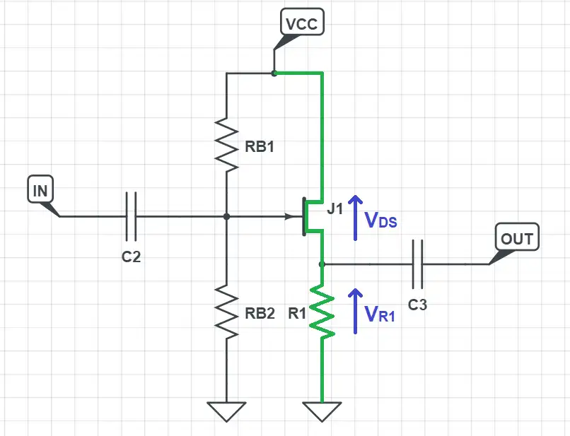
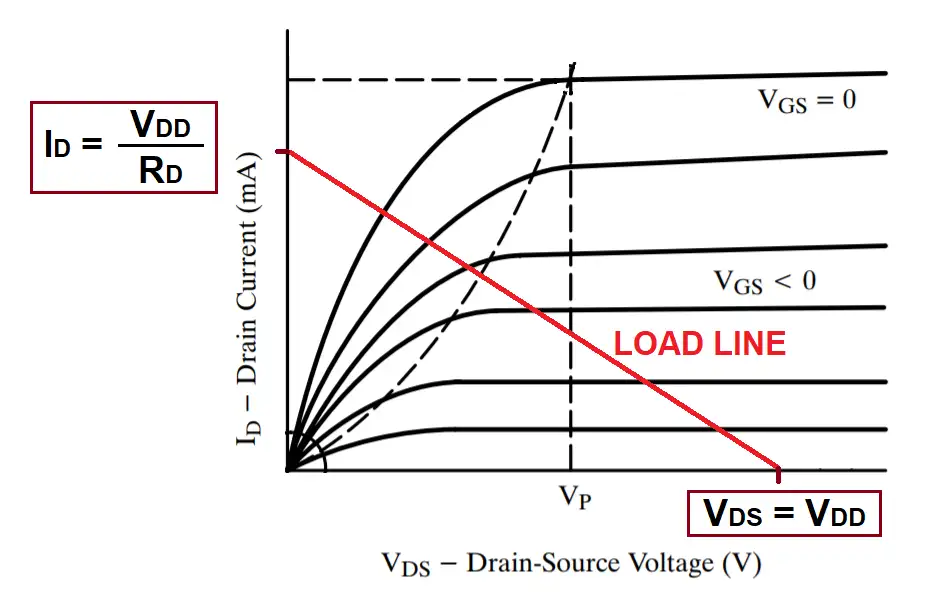
Similarly as we did with the BJT transistor, when analyzing a JFET design you’ll often want to draw the load line. This line contains all the possible working points of the transistor in a given circuit, and it’s extremely useful to find the Q-point where the transistor is biased.
By applying Kirchoff’s voltage law in the branch that goes from VCC through the transistor, R1 and ends in ground, we get:
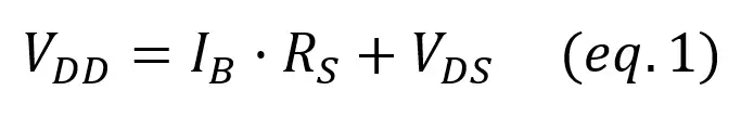
This is a line equation of the form y = a·x + b, so if we get two points we can draw the line. To find these points we can choose any condition we want, so we’ll pick the two that are easier to figure out:
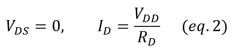
Point 1: we make Vds = 0. If Vds = 0, all the voltage is dropped at the resistor and we can get the current value thanks to Ohm’s Law:
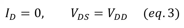
Point 2: we make Id = 0. If no current flows through the circuit there’s no voltage drop at the resistor (V = I·R) and all the voltage is dropped at the transistor:
Now we can draw the load line over the characteristic curves. As the gate voltage (Vg) is 4.5V, the Q point will be the intersection of the load line with the curve Vg = 4.5V.
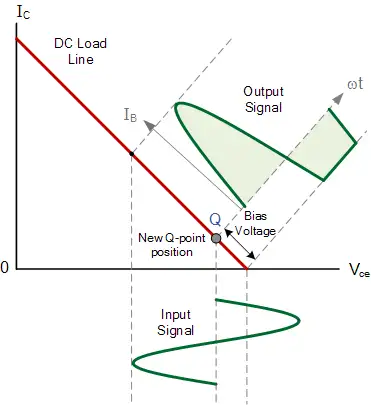
Our Q point will be the “no input signal” response from our JFET amplifier, and we will have a constant output. When our instrument signal is connected to the input the output will begin to swing around this point:
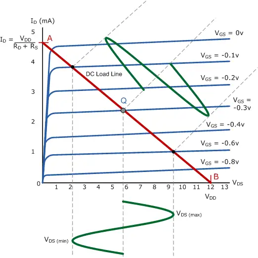
When designing an amplifier the parts have to be chosen so the working point is around the middle of the load line. If we set it too next of one of the sides, the signal won’t be able to swing properly and there will be unwanted distortion:
2 – JFET Application Circuits
2.1 – Switch
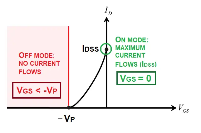
As a JFET is a device that controls the amount of current going through it via an input voltage, the first application circuit is obvious: a switch. In our effect pedal kits we take advantage of the 3PDT to turn the led on and off mechanically, but a circuit like the following one could perfectly be used instead:
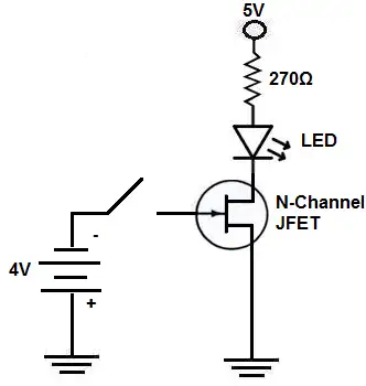
If we apply a voltage Vg < Vpinchoff, the transistor will act as an open switch and no current will flow (Id = 0). If Vg = 0, the maximum current will flow through it (Id = Idss) like if it was a closed switch. This can be observed graphically with the following chart you can get from the JFET datasheet:
2.2 – BUFFER
JFET buffers are one of the easiest circuits you can build with these transistors and are a great beginner project if you’re starting building your own circuits. [As we reviewed in our buffer post] these circuits are designed to provide huge input impedance, so what better than a JFET with hundreds of thousands of Megaohms?
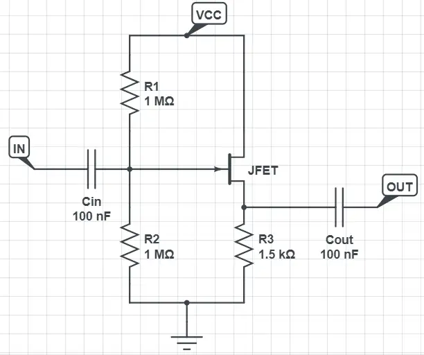
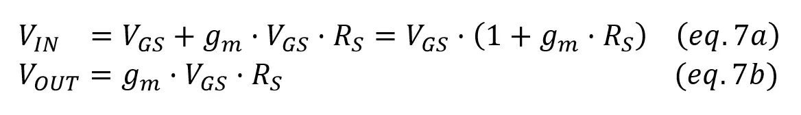
The JFET transistor is used in what’s known as common drain configuration (or source follower), and it only uses three resistors and two capacitors to create a mirror of the input signal in the output of the circuit. The setting is as follows:
- The Gate pin of the transistor acts as the input
- The Source pin of the transistor acts as the output
- The Drain pin of the transistor acts as the common (connected to VDD).
Cin and Cout just act as coupling capacitors (so no DC goes in or out the amplifier), but they are not necessary for the analysis.
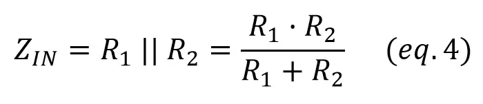
Input impedance:
As the JFET has a huge impedance compared to anything connected to it, the input impedance will be determined only by the resistors we connect to it:
With Kirchoff’s Voltage Law,
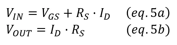
Substituing the JFET formula we saw in our previous post,
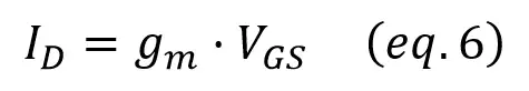
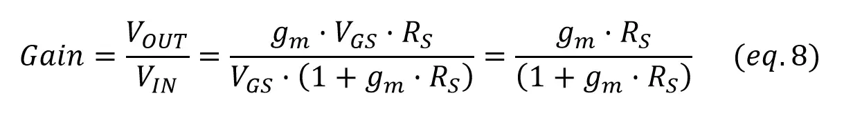
gm is the gain of the transistor, which has high values, and Rs has values of at least 1kΩ: when we multiply the two of them we get a very high number, so adding 1 to this number won’t change much.
Let’s prove it with an example. If we take 1000000 as our high number, adding 1 doesn’t make a big difference. In the gain ratio of the equation 8, 100000/100001 = 0.999999 ~ 1.
The result is that we can approximate 1 + gm·Rs ~ gm·Rs.
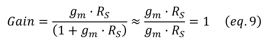
That’s why this circuit acts as a buffer: the output voltage will always follow the input voltage.
2.3 – VOLTAGE CONTROLLED RESISTOR
One very interesting JFET application is the use as a voltage-controlled resistor. This is achieved by setting a Q point in the ohmic zone. For amplifiers we have to set it in the saturation (or active) zone, because we want our output to be only related to the input voltage: no matter what the Vds is, for a given Vg the output current will remain practically constant. The saturation region is represented in red in the schematic below.
However, in the ohmic region (green) things are way different: if the Vds varies, the current varies almost in a linear way with it which remembers quite much to the resistor voltage vs current equation:
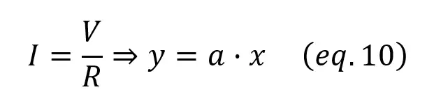
In this case, a (the slope of the line) = 1/R, so by varying the gate voltage we can change the value of the equivalent resistor created by the JFET.
Some effect pedals like the MXR Phase 45 and the MXR Phase 90 take advantage of this phenomenon and use them in their filtering:
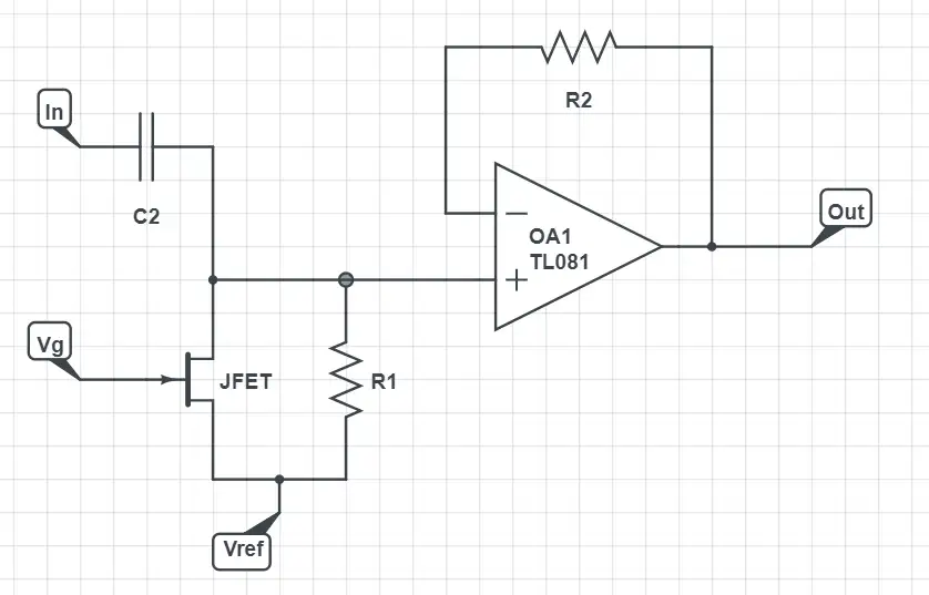
With this configuration, the value of the equivalent resistor can be easily changed if the output of a low frequency oscillator is applied to the gate of the transistor. As the resistor value controls the filtering, with a varying voltage we can create the phase effect. Let’s see an example to make it clearer:
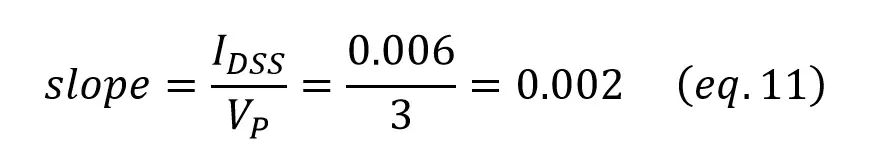
For the last picture, the values are:
Idss = 6mA
Vp = 3V
First of all we have to assume that in the ohmic region the response is a straight line (this is quite true in most devices).
As slope = 1/R,
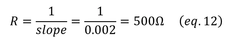
We could do this with every value of Vgs, and we would get the equivalent resistor corresponding to each value.