Electronic Components, Electronics Tutorials, Transistors
Electronics Tutorials: the JFET (I) – Basic concepts
JFETs are commonly used in effect pedal circuits. Keep reading and learn why!
In this post we’ll explain the basic principles of operation behind Junction Field Effect Transistors: how do a JFET work, what characteristics make them attractive to build circuits and much more. While we’ll keep it as light as possible some theory may be thrown here and there, so don’t be afraid if you find some sections a bit dense. Let’s start!
1 – Introduction
The JFET (Junction gate Field Effect Transistor) is a semiconductor device. JFETs have three terminals: Gate, Source and Drain.

Whereas the physical principle behind JFETs is different than the one behind BJTs, they work in a similar way. To understand how a JFET works you just have to imagine a hallway with a door in the middle, and people trying to go from one side to the other. If the door is completely open more people will be able to go through, and this number will decrease as the door is more and more closed. In our example, the corridor would be the internal connection between Drain and Source terminals, people would be the current flowing through the transistor and the Gate the control of how much the door is open. This explanation should make evident why JFETs are very good to control the amount of current that goes through them. This is how a JFET is internally designed:
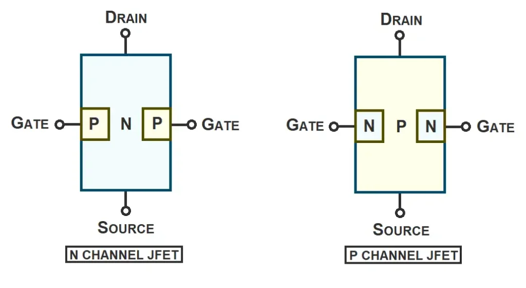
The basic layout is a sandwich of P and N materials. The middle material (the part that connects the Drain to the Source) is the channel of the transistor: if this middle material is N-type the JFET is an N-channel transistor and if it’s P-type it’s a P-channel transistor. As you can see in the picture above, JFETs are quite symmetrical, so the question is obvious: can I switch the Drain and Source pins? This is possible in many cases, but JFET manufacturers optimize their transistors to be used in one direction. That way you’ll get the most out of your JFETs, like better gain or input impedance.
2 – JFET Principle of operation
JFET are voltage controlled devices (if you remember from our BJT post, bipolar transistors are current controlled instead). This means that the amount of current that flows through them is controlled only with the voltage applied to the Gate terminal but there’s no need for a bias current as it happens with BJTs. [jfet-gate-voltage-channel.jpg] When the voltage in the gate increases, the conduction channel is restricted and the current that flows through the device decreases. When the voltage applied reaches a certain amount the “door” is completely closed and no current flows through the JFET. This is known as the pinch off voltage. [jfet-gate-voltage-pinched-channel.jpg] Remember there’s two kinds of JFETs, N-channel and P-channel? For an N-channel JFET the voltage we have to apply in the Gate must be lower than the one we apply in the Source while in a P-channel JFET this voltage must be higher. This is because we want to reverse-bias the P-N junction; otherwise the JFET would act as a diode and not as a transistor.
3 – Important parameters
3.1 – Gain
The relationship between the input voltage and the output current is given by the formula:
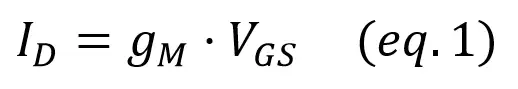
Gm is known as transconductance, and is one of the most important JFET parameters. It relates how much current will flow depending on the Gate voltage Vgs. This formula will probably sound familiar to you, as it’s very similar to the BJT gain formula.
3.2 – Input Impedance
In their standard use (Gate is the input) JFETs have a huge input impedance. This make them very suitable to build buffers or input stages as they prevent tone loss. As an example, the J113 JFET transistors we use in many of our effect pedal kits have an input impedance in the range of 1.000.000.000~10.000.000.000 ohms.
3.3 – Maximum current
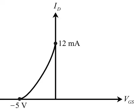
This is the maximum current the JFET can let through when the resistive channel is fully open. If it’s an N-channel JFET, this happens when the Gate-Source voltage is zero. This maximum current value is known as Idss.
3.4 – Regions of the JFET
JFET characteristic curves, like the ones below, represent how the JFET works under different situations. These graphical tools are available from the manufacturer’s datasheet and are extremely useful: they allow you to make a quick analysis and have an idea about how the JFET will behave.
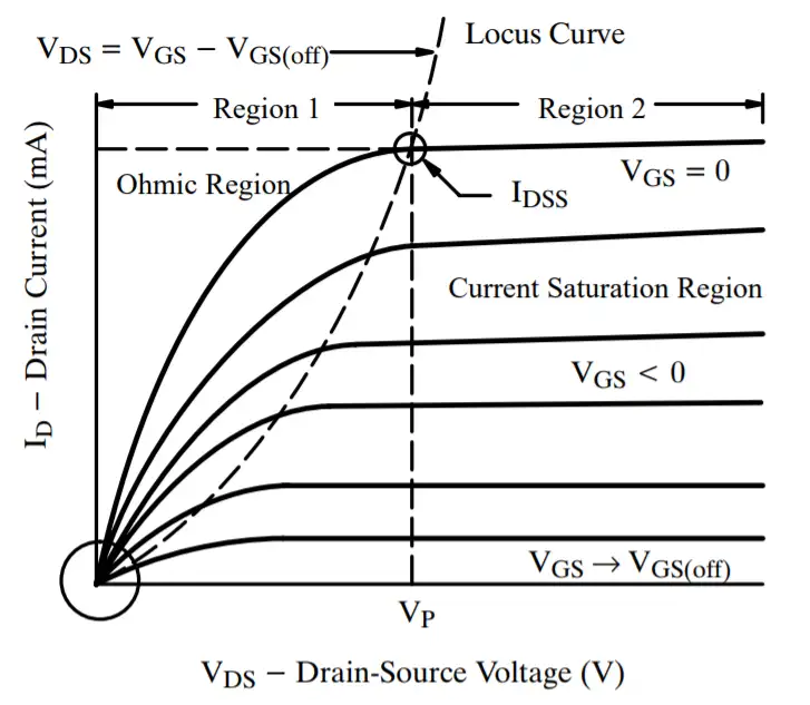
Depending on the area of the graphic we’re on the JFET will operate in a different working mode:
– Pinch Off Region: this is the “Off Mode” of the transistor. The channel is fully pinched because of the voltage applied to the gate, and no current is allowed to flow through the JFET.
– Ohmic Region: here the JFET acts as a variable resistor which resistance can be controlled with Vgs. The current through it is almost linear depending on the voltage applied to the transistor:
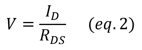
This zone is not very useful to design amplifiers as the current depends from the Gate control
– Saturation or Active Region: when operating in this zone the JFET is a good conductor. The current is only controlled by the Vgs voltage, making it the perfect region to design amplifiers.
[dibujo recopilatorio con canal en cada una de las zonas]
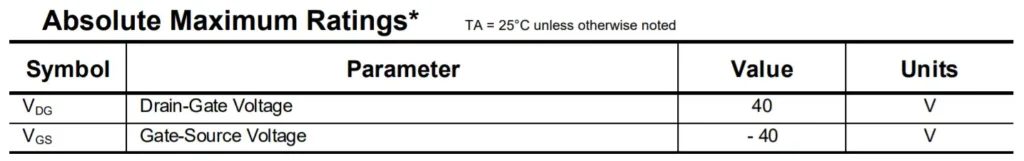
– Breakdown Region: if the voltage between the pins exceeds a certain value the resistive channel breaks and the JFET becomes a short circuit, being unable of any kind of current control. This is irreversible: once it goes into the breakdown region the JFET gets permanently damaged.
The maximum voltage allowed can be found in the transistor’s datasheet and should never be exceeded:
Now that you’ve grasped the basics of JFET transistors, in the next post we’ll cover circuit analysis and design!