Effect Pedal Circuits
Effect pedal circuits: the Buffer
Audio buffers provide a high input impedance for the audio signal and a low output impedance, meaning that they can drive circuits or pedals that require more current without degrading your audio signal. In a simple way, they take your “weak” input signal (maybe because of long wires, high output impedance…) and transform it in a strong signal that won’t degrade easily. Dive in and learn more about them!
1 – Introduction to buffers
First of all, there’s two kinds of buffer: current buffers and voltage buffers. For small signal audio we’re more interested in voltage buffers as we represent audio as a voltage signal, so we’ll use the term “buffer” to refer to voltage buffers from now on.
A buffer is used to take the input signal source and transform it from one circuit to another, making it more robust and prevent it to be altered. In voltage sources, we have a problem when a load (may that be the following pedals, the rest of the circuit…) requires too much current. That happens for example in old fuzz pedals that had very low input impedance: we say that they “load” the guitar pickups because they require a high amount of current to work, and this high current can modify the shape of the sound.
To avoid this problem we use a buffer. In our case it’s a circuit with the following characteristics:
- a very high input impedance that won’t let almost any current to flow, preventing the sound to be degraded
- a very low output impedance that will be able to feed a very high current in case the following circuit needs it while preventing the sound to be modified
Ideally our voltage buffer will have infinite input impedance (zero input current) and zero output impedance. As we don’t want to change the signal volume we’ll be looking for a circuit with no gain, or with gain = 1. So now that we have an idea of what we’ll ask from the circuit, let’s check some buffer examples!
2 – JFET BUFFER
JFET Buffers are one of the easiest circuits you can build and are a great beginner project if you’re starting building your own circuits. To understand how they work, we’ll take a look at the circuit of our JFET buffer kit. Don’t miss our JFET post to learn more about these useful devices!
2.1 – Input
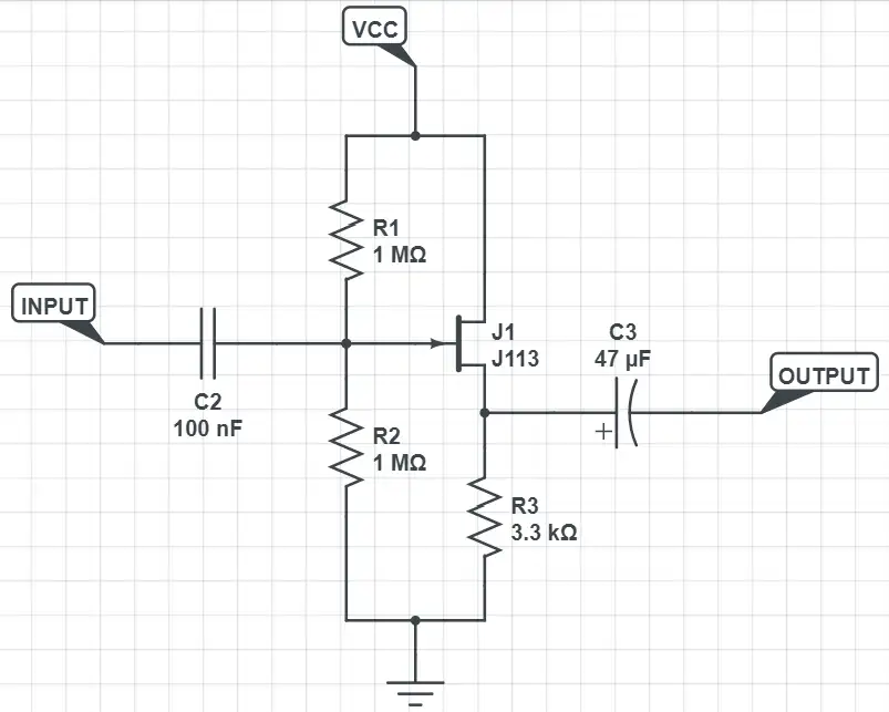
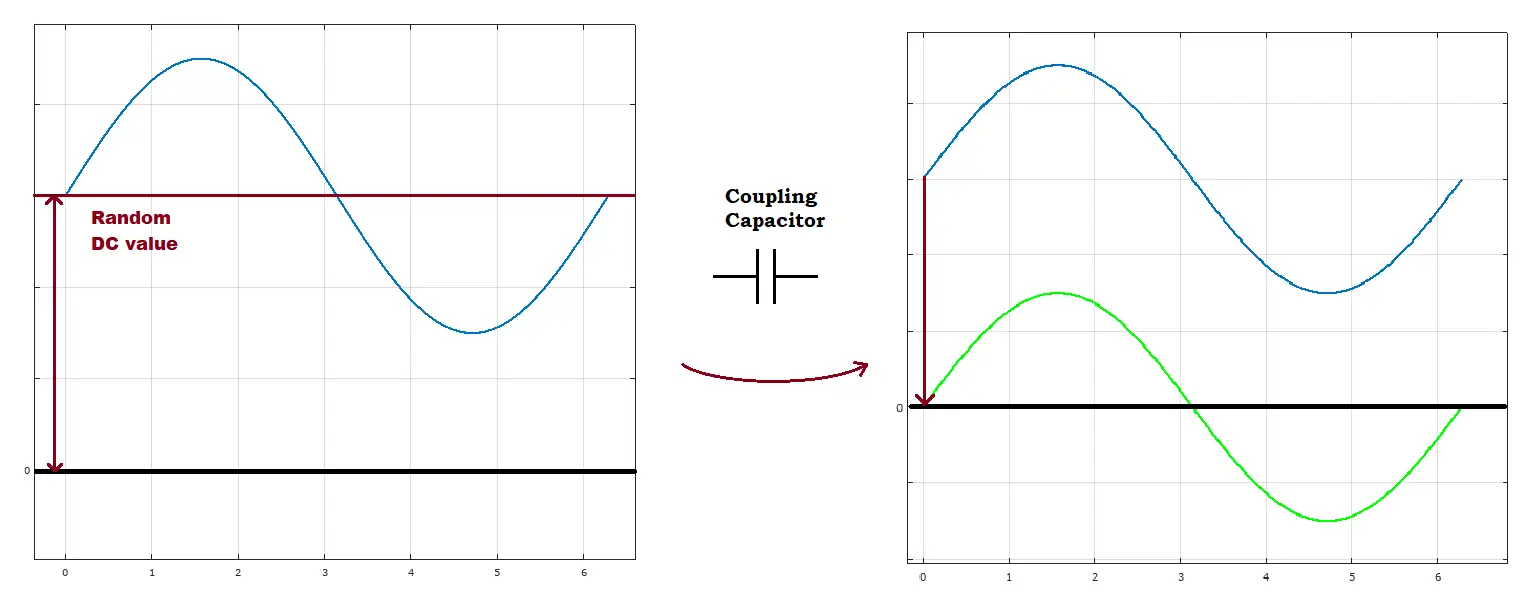
C1 is called a coupling capacitor and is used to block the arbitrary DC part of the signal. Usually audio signals have two parts:
- An AC alternating signal: this is the one we are interested in as it is the one that carries the audio information
- A DC constant part that doesn’t provide any information and can make our buffer not to work properly.
By using a coupling capacitor we are able to remove the DC part and keep only the pure AC audio signal.
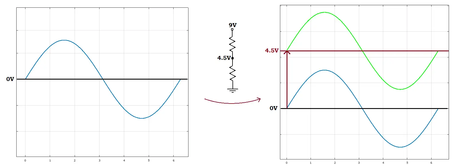
After that, R1 and R2 are used to create a voltage divider of half the input power (typically 4.5V) that is added to our AC signal. Active electronic devices can only work between the power supply voltages: a transistor powered between 0V-9V can only amplify from 0V to 9V. As input audio signals from your instrument are symmetric (they swing from positive to negative voltages) and your DC source is only positive, you need to add a bias voltage to your audio signal. That way the signal remains between 0V and 9V:
As the JFET input impedance can be considered almost infinite, the JFET buffer input impedance is determined by R1 || R2, in this case 500k.
2.2 – AMPLIFICATION STAGE
Our JFET buffer uses a JFET transistor as active element, and it only uses three resistors and two capacitors to create a mirror of the input signal in the output of the circuit. Buffers are a particularization of an amplifier with a gain of 1, that’s why this is known as amplification stage even if the output signal is the same as the input.
The JFET transistor is used in what’s known as common drain configuration or source follower. The setting is as follows:
- The Gate pin of the transistor acts as the input
- The Source pin of the transistor acts as the output3
- The Drain pin of the transistor acts as the common (connected to VDD).
If you want an in depth analysis of the JFET equations and gain calculation don’t miss this post!
2.3 – OUTPUT STAGE
As in the input stage, a coupling capacitor is used to prevent any DC that might have generated in the amplification stage to go outside of the buffer, as we’re only looking for a clean AC signal.
And that’s it for our JFET buffer! Now let’s have a look at another common circuit: the OpAmp buffer.
3 – OPAMP BUFFER
OpAmps are great to build buffers as they have a huge input impedance and are very stable: JFET circuits will have to be retuned if you swap the original transistor for another model (and even for the same model of another batch!). This happens in general for any transistor-based circuit.
On the other hand, you can safely replace your JRC4558 for a TL072 or an LM358 and your design will work the same way. Okay, for some people maybe the sound “color” changes a bit, but the circuit will behave the same way and will have the same gain and frequency response. Here you can find an introduction to OpAmps and basic concepts.
We’ll use our opamp buffer kit circuit to analize how a opamp based buffer works!
3.1 – Input Stage
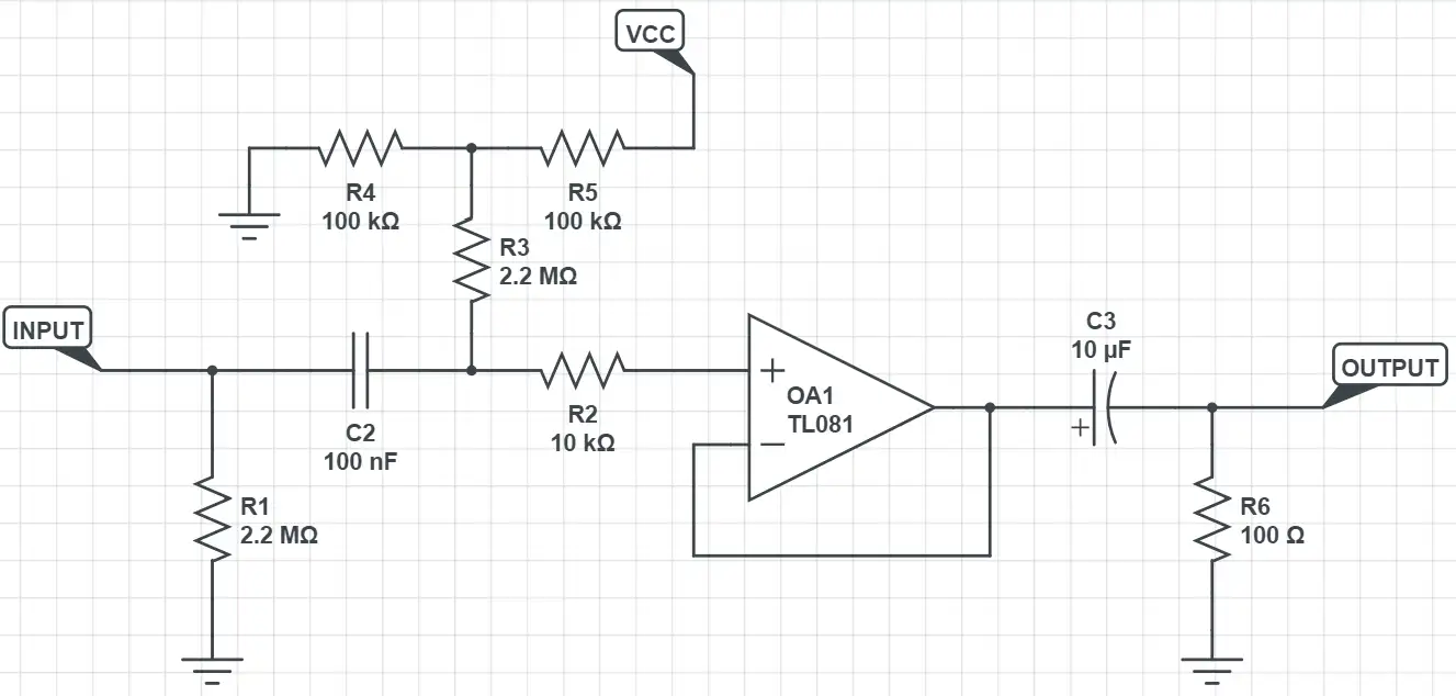
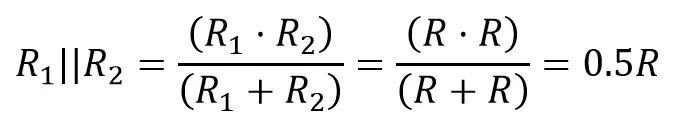
As in our JFET buffer, our input buffer has a DC coupling capacitor (used to avoid any input DC voltage, as the audio signal we want to amplify is only AC). To add a voltage of half our DC supply, we use two resistors (R1 and R2). Their parallel equivalent R1||R2 will determine the input impedance of the buffer. As they have the same value R, the input impedance is given by:
3.2 – Active stage
Our opamp is set with a negative feedback topology, the one that is used in most cases. As opamps have huge open loop gain values (easily more than 1000000, and noted as Aol), negative feedback is needed to have a controlled gain device. The basic opamp analysis equation is:
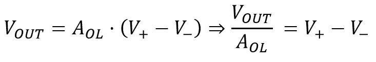
From our OpAmp post you’ll remember that V+ and V- can be considered to be exactly the same.
For analysis, we assume Aol = ∞
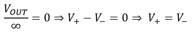
As in our circuit V- = Vout, our output voltage is the same than the input voltage: Vin = Vout
3.3 – Output stage
Another DC coupling capacitor prevents any DC that might appear in our signal to be blocked before sending the signal to the output of the circuit.
Buffers are highly recommended as they help to keep your sound signal unaltered through the pedal chain. The JFET buffer and the OpAmp buffer are two of the most common circuits and are a very easy to build, so they’re a great project if you are starting into electronics!