Effect Pedal Circuits, Electronic Components, Electronics Tutorials, Transistors
Electronics Tutorials: The BJT Transistor (II)
In the last post we introduced a widely used device in effect pedals: the BJT transistor. Now we’ll look at some useful circuits and how they are designed: amplifiers, switches and more!
1 – Current Loops Analysis
To explain the next concepts we’ll use the following circuit as a guideline:
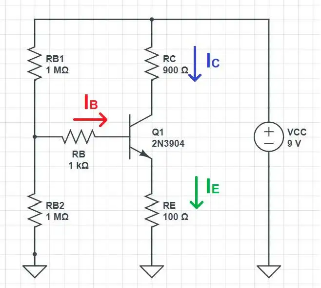
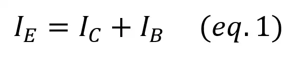
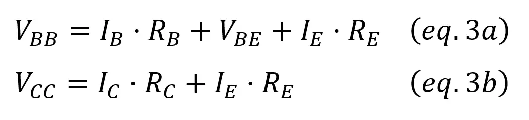
First of all, from this first schematic we can get the most important relation when analyzing a bipolar transistor circuit. The amount of current going into the transistor must equal the amount of current going out (Kirchoff Current Law):
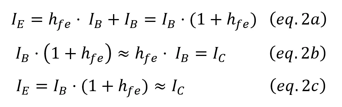
In general this equation can be simplified as the gain of a transistor is very high. This means (hfe + 1) ~ hfe. We’ll use this approximation in the rest of the explanation to make things easier, but the complete formula can be used instead. The other simplification we’ll do is the resistor voltage divider: these resistors act as a constant voltage for the base. As they have the same value, this voltage is VCC/2 = 4.5V.
Now Kirchoff’s Laws can be used with the following loops:
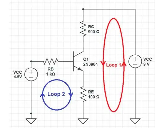
As the voltage across a closed loop must be 0,
From these equations, we can get the values of resistors for the desired amount of current. But how much current do we need? Keep reading!
2 – BJT transistor biasing
A bipolar transistor doesn’t work by just connecting the output of your guitar to it: you have to add a few parts and power signals to place it in a “sweet spot” or Q point (quiescent point) where it can work. This is known as transistor biasing. These extra parts set the DC operating point correctly so the input signal will make the transistor work as intended.
The process to design an amplifier can be summed up in the next two steps:
- Drawing the load line, that is the line that contains every possible working point for the transistor in our circuit.
- Choose the best possible Q point for our application. In our case we want the transistor to amplify so we need pick a Q point in the active region.
We’ll use the following circuit for this section:
1 – The load line
The load line is a very useful tool when designing bjt amplifiers. It indicates all the possible Q points in which the transistor can work in a given circuit. Once we have the load line for our circuit, we’ll pick the best available Q point. In the next picture the load line is painted in red, the x axis represents Vce and the y axis represents Ic.
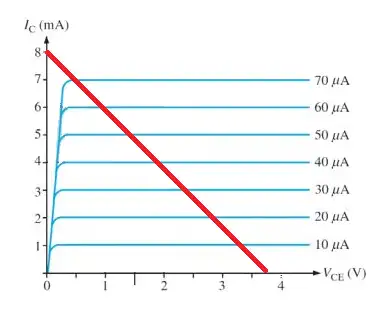
To get a straight line only two points are needed, so we need two conditions. We can choose anything we want so we’ll take the two that are easier to solve:
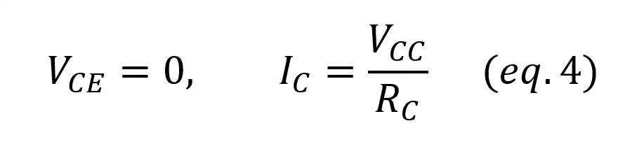
- If Vce = 0 the transistor is in the saturation region so we have maximum current. As the transistor acts as a closed switch, the current is limited only by the resistor. This is our first point of the line:
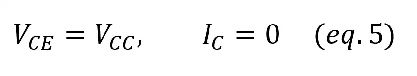
- If Ic = 0 no current is flowing. This means that there’s no voltage drop in the resistor (V = I·R) and all the voltage drops in the transistor (Vce = Vcc). Now we have our second point:
With our two points we can draw our load line, that contains all the possible working points for the transistor.
2 – Choosing a Q point
As we said earlier the Q point should be in the active region, but where exactly? If you look for the quick answer, in the middle of the load line.
Now comes the detailed explanation. The Q point represents the state of the transistor in “standby”, when no input signal is applied. When we connect our instrument to the input, the Q point will swing around this standby point following the input signal:
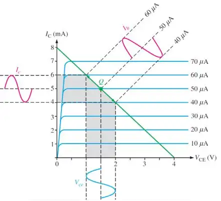
We want our transistor to amplify with the maximum possible swing without entering in the cutout or saturation region, so we have to choose a Q point in the middle of the load line.
Once the Q point has been chosen we can find graphically the values of Ic and Vce.
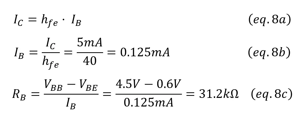
2 – Resistor Calculation
By now we have all we need to obtain the resistor values!
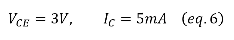
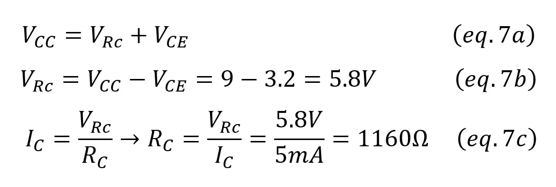
- Ic = 5mA and Vce = 3V. From this condition we can get Rc. To do so we follow these steps:
1 – calculate the voltage drop in the resistor (eq. 6b) 2 – calculate Ic (eq. 6c)
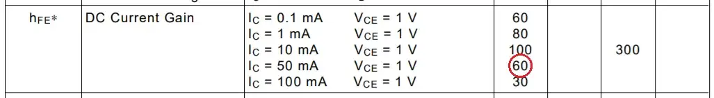
- Ic = hfe·Ib. With this equation we can calculate the base current we need. The hfe or gain value depends on the transistor and can be obtained from its datasheet. In this case, hfe = 40.
With this value we can analyse the loop 1 in our example circuit using Kirchoff’s voltage law:
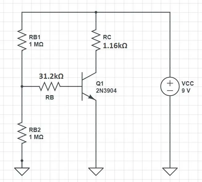
Here’s the final circuit to meet our design specifications:
APPLICATION CIRCUITS
APPLICATION CIRCUITS
3 – Application Circuits
Here are covered another kind of circuits using bjt transistors that you can find in [effect pedal circuits]: the common collector buffer and the switch.
3.1 – COMMON COLLECTOR BUFFER
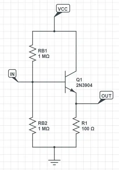
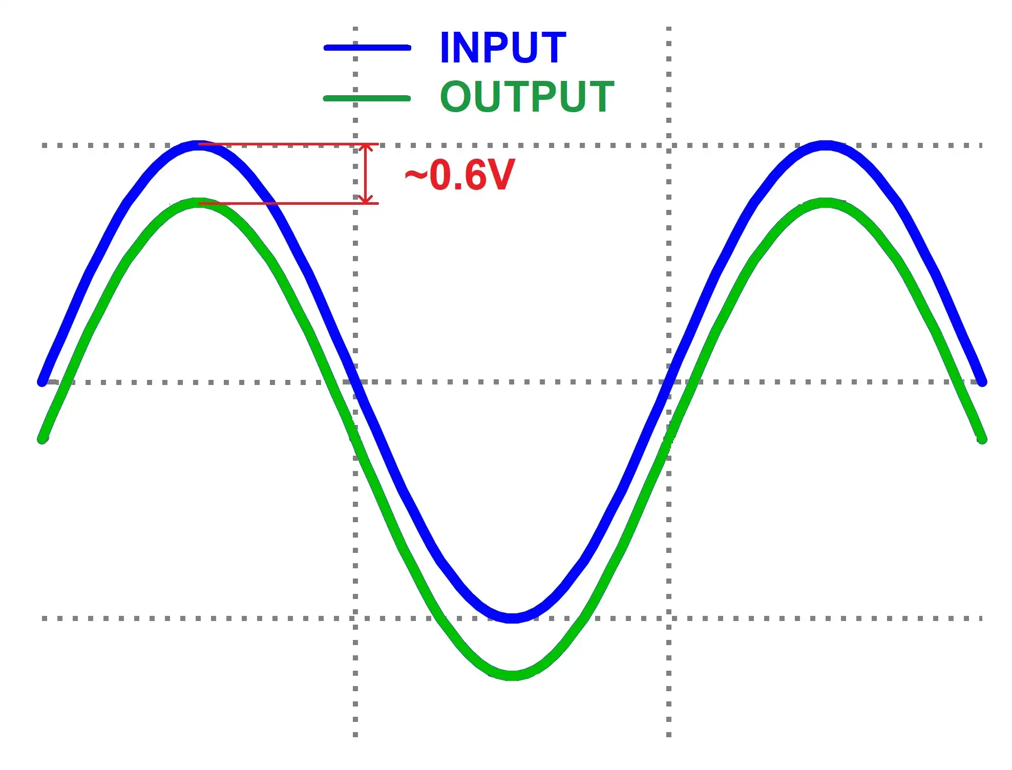
In the common collector mode the collector is directly tied to Vcc, and a resistor is placed between the emitter and ground. As there’s a diode union between the base and the emitter, the voltage at the emitter always follows the base input voltage minus the forward voltage (~0.6V).
The bipolar transistor is an alternative to the JFET or OpAmp buffers, but as it has a lower input impedance it’s not used that often.
3.2 – Switch
Another common use for the BJT transistor is as a switch. In our effect pedal kits we always include a True Bypass footswitch to toggle the effect and LED on and off, but in other pedals a BJT is used as a switch for this purpose.
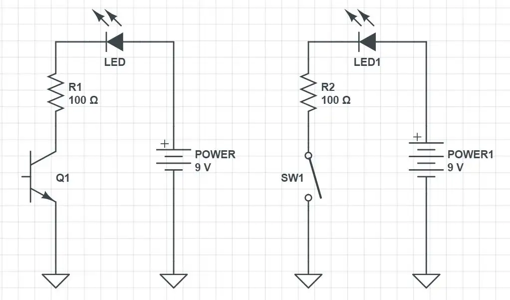
When a voltage is applied to the base of the transistor the bjt acts as a closed switch: the current can flow and the LED is turned on. When the voltage is removed the BTJ acts as an open switch, and no current can flow: the led is turned off.
If you’ve missed the previous post, we recommend you to check it. You’ll find an introduction about BJT Transistors and some very useful concepts that will allow you to better understand these devices: