Electronics Tutorials
Electronics Tutorials: The BJT Transistor (I)

Oct
You’ve probably encountered references like bipolar transistor, BJT, PNP or NPN transistor. After reading this post, these terms will have no mistery for you!
Introduction
Introduction
The bjt transistor was invented in 1947 at the Bell Labs, and provoked a huge inflexion point. In the special case of music electronics, the BJT started replacing a device most musicians love: the vacuum tube.
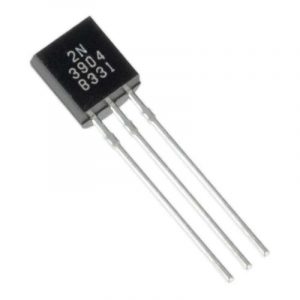
BJT or bipolar transistors are widely used in [effect pedal kits and circuits] along with [JFET transistors]. Its name stands for Bipolar Junction Transistor and it is one kind of semiconductor device. In many modern applications like computer microprocessors there’s a huge number of transistors per IC (more than 1 billion!), but for effect pedal kits we use discrete transistors: each IC contains only one BJT. In the following picture you can see one of the most used BJT transistors: the 2N3904.
If some of the nomenclature used in this post seems confusing to you, take a look at the [first section of our post about Diodes]. It’s a quick introduction to semiconductor devices and basic concepts like p-type and n-type materials or how they can be combined.
How do BJTs work?
How do BJTs work?
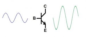
A BJT transistor has three terminals: emitter, collector and base. The working principle behind BJTs can be easily explained: imagine a hallway with a big door, and people trying to go from one side to the other. The more you open the door the faster can people pass through.
In this example, the emitter and collector would be the two sides of the hall, and the base the door opening control. This is what bipolar transistors do: they have the ability to control the current that flows through them. But while [in JFETs this “opening” is voltage controlled] in BJTs the current flow is controlled by a current. The most interesting part is that this control current is very small compared to the current flowing through the BJT, and that this small current and the bigger current share the same shape: that’s the basic principle behind an amplifier!
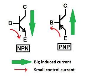
Internally, a BJT is made as a 3 layer sandwich of p-type and n-type materials. If the outer layers are n-type the BJT is NPN and if the outer layers are p-type it’s a PNP:
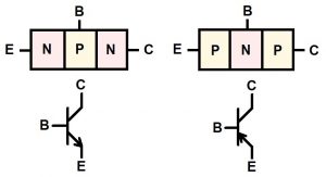
What’s the difference between the two types? As we explained in [our post about Diodes] P and N materials are basically silicon with an excess of either positive or negative charges. These charges are responsible for the current conduction, as bare silicon is not very conductive. NPN and PNP work the same way, but the charges that carry the current are opposed. That’s why on NPN current flows from collector to emitter and in PNP it’s the other way around. Even if they look symmetrical, bipolar transistors should always be connected respecting the polarity of emitter and collector: internally, the device is not perfectly symmetrical and is optimized to work in one way.
BJT Characteristics
BJT Characteristics
1 – Current flow
BJT transistors are current controlled: the amount of current going through the base determines the amount of current flowing between the emitter and the collector: The more current flows into the base, the more current will the transistor drive between emitter and collector.
Internally, the transistor is very similar to another semiconductor device: [the diode].
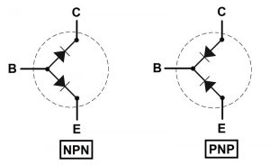
If you compare this against the transistor symbol, you’ll find that the arrow in the lower junction (the one between the base and the emitter) matches the direction of the arrow in the symbol. To remember how current flows in BJT transistors you just have to remember this one tip: the small arrow in the BJT symbol lets you know the current flow direction!
2 – BJT gain
So far we’ve seen how with a small current we can control a big current flow. But how “small” is small and how are both currents related? The relation between the two is given by one of the most important transistor parameters: the gain. The current going into the base, Ib, and the collector current, Ic, are related through the transistor gain (also known as hfe):
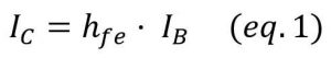
This is one of the most important parameters when doing a BJT design, as it tells you how much the output signal will be amplified.
3 – Zones of operation
If we take the 2-diode model for the BJT, we have up to 4 different possibilities depending on the polarity of each junction. These are known as the 4 transistor operation zones.
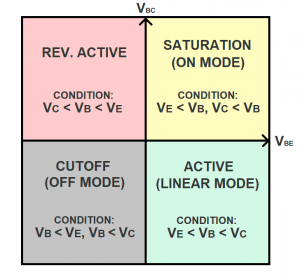
- Cutoff region, also known as off mode. The two diodes of the equivalent model are reverse biased and thus there is no current conduction: the transistor acts as an open switch and no current will flow between the collector and the emitter.
- Saturation region. This zone is the On mode of the transistor, that acts like a closed switch between collector and emitter. The base current has exceeded the point where it can control the voltage between the collector and the emitter is < 0.2V no matter the current. In the equivalent model, the two diodes are forward biased.
- Active region. This is where the amplification magic happens, and it’s the zone in which you’ll want your transistor to work.
- Reverse active region. Remember the fact that bipolar transistors are symmetrical, meaning that they should work when connected backwards? Well, we’re in this case. In the reverse active mode the transistor acts like in active mode (it amplifies the incoming signal) but the gain is much lower.
Keep reading more about BJT Transistors in the next post: